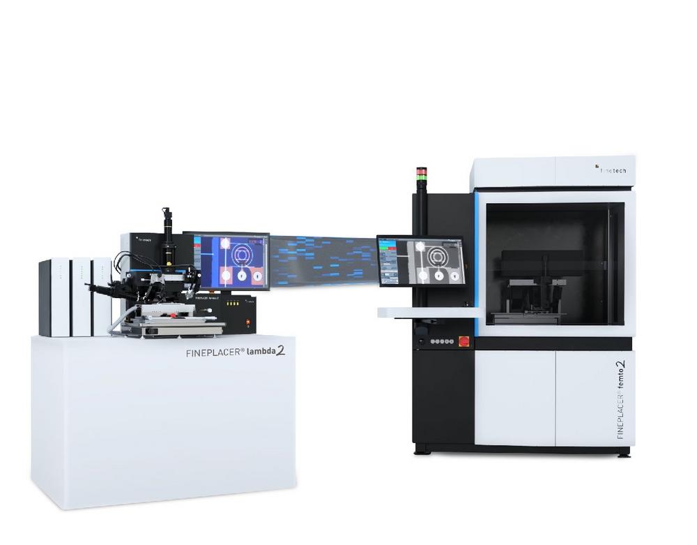
Finetech has been supporting start-ups as well as global technology leaders for three decades in the development of innovative semiconductor products. The highly accurate sub-micron placement and assembly systems are a cornerstone of the Berlin-based mechanical engineering company’s portfolio – valued worldwide as versatile, cost-efficient and compact bonding platforms for R&D, prototyping and automated production.
They are the first choice for complex multi-stage assemblies with very high accuracy requirements, as well as diverse and demanding bonding technologies. Applications include the development and production of optical transceivers up to 800G and beyond for data communication, environmental sensors for autonomous driving, the integration of micro-optical components for novel quantum sensors, or power laser modules for use in industrial and medical applications.
FINEPLACER® lambda 2 – the starting point for successful product development
For basic research, development and prototyping, Finetech offers manual and partially motorized table-top systems. At the forefront is Finetech’s successful manual sub-micron die bonder FINEPLACER® lambda 2.
The FINEPLACER® lambda 2 is used to place and connect components with an accuracy of better than 0.5 microns – ideal for the requirements, e.g. in the development of opto-electronic products such as transceivers (TOSA/ROSA) or laser diode modules.
Thanks to the proven FINEPLACER® alignment and placement principle with only one moving axis, the system combines highest process quality, stability and accuracy. In conjunction with specially developed optical systems with an optical resolutions down to 0.7 µm, it enables superimposed images of the highest optical quality for the reliable detection and alignment of finest structures in the micron range.
The FINEPLACER® lambda 2 was designed with particular focus on the user’s needs. Thanks to the ergonomic machine design and software-supported guidance, the operator always remains at the center of the action. All operating elements have been adapted to the typical workflow. This allows the user to concentrate on the essentials and quickly obtain results. The uniform operating concept with clearly structured process sequences also ensures quick familiarization.
“Prototype-to-Production” allows seamless process transfer to automated FINEPLACER® femto 2
Placement and assembly processes can be automated quickly and easily on Finetech equipment. This is enabled by Finetechs "Prototype to Production" approach based on a fully integrated technological ecosystem. Since all new die generation die bonding systems by Finetech share the same cross-system machine architecture, a unified process module platform, and identical software and operation, it is possible to consider all future automation steps as early as the development stage and then transfer qualified development processes in all their technological diversity to the production environment.
Finetechs "Prototype-to-Production" approach enables fast, creative and flexible product development with a comparatively low initial investment and minimized technological risk to support an efficient realization of product ideas.
For users of the FINEPLACER® lambda 2 who want to transition their product innovation into the manufacturing stage, Finetechs automated die bonder FINEPLACER® femto 2 is the logical next step as it maintains the level of reproducibility and accuracy of the processes developed on the FINEPLACER® lambda 2, while at the same time integrating the automatic handling and process steps required for series production.
The automatic bonding platform offers placement accuracy down to 0.3 micron @ 3 Sigma and supports a wide range of assembly applications at chip and wafer level. Designed for complex applications with highest accuracy requirements and a diverse technology mix, the system is suitable for automated development environments, as well as high-yield manufacturing of high-quality semiconductor products.
The Vision Alignment System FPXVisionTM allows cost- and time-efficient passive optical placement of devices. In combination with a powerful pattern recognition, it opens up numerous possibilities for the user in terms of application flexibility and accuracy.
The FINEPLACER® femto 2 has a special housing to eliminate external interference factors and to precisely control and influence the process conditions. Filter technology ensures a protected process environment in cleanroom quality up to class 100/ISO 5 – regardless of the machine’s location.
Flexibility and compatibility
The FINEPLACER® lambda 2 and FINEPLACER® femto 2 both support individual configurations. The modular architecture of the FINEPLACER® platform makes it possible to equip the machine with a multitude of extension modules for a wide range of assembly and bonding technologies, including eutectic soldering, thermocompression bonding or bonding with UV-curing adhesives. This technological diversity opens up a wide range of applications, which can be further expanded by the large bonding force range.
The systems remain adaptable at any time: if the technology requirements change, the corresponding process module can be retrofitted by the user via plug & play.
Process development and automated production cannot be more flexible; at the same time follow-up costs are kept low and the investment is safeguarded even with changing application requirements. Ideal for users who frequently want to implement new technologies and processes in the long term.
The FINEPLACER® lambda 2 will be exhibited at LASER World of Photonics Munich 2022, hall B5, booth 327.
Finetech is a developer and manufacturer of innovative equipment solutions for a variety of SMD rework and micro assembly applications. Due to their modular architecture, the manual, semi-automated and full-automatic systems offer maximum process flexibility. Typical fields of use range from R&D and prototyping (high accuracy, low volume) to fully-automated production environments with high yield.
Finetech’s customers include companies in the aerospace, automobile, medical/bio/solar technology, optoelectronics, semiconductor, consumer electronics and defense sectors, together with education and research establishments. Finetech responds flexibly to specific requirements and offers tailor-made solutions to highly-demanding customer applications. The company is represented by direct subsidiaries in its core markets and offers on-site application support and advice. It is also represented world-wide by a network of agencies.
Finetech is headquartered in Berlin, with subsidiaries in Arizona, New Hampshire, Shanghai, and Tokyo.
FINETECH GmbH & Co. KG
Boxberger Str. 14
12681 Berlin
Telefon: +49-30-936681-0
Telefax: +49-30-936681-144
http://www.finetech.de
Manager Marketing Communications
Telefon: +49 (30) 936681-331
Fax: +49 (30) 936681-144
E-Mail: tobias.gleichmann@finetech.de
Marketing
Telefon: +49 (30) 936681-330
Fax: +49 (30) 936681-45
E-Mail: daniel.staubach@finetech.de
![]()

